
Can hdi pcbs be used in automotive applications?
Can hdi pcbs be used
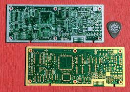
Printed circuit boards (PCBs) are crucial in controlling the many electronics in modern vehicles. They are also responsible for many of the vehicle’s advanced features such as entertainment and navigation systems, GPS and engine management systems. The PCBs found in today’s vehicles must be able to withstand vibrations, high temperatures and harsh environments. As such, the industry has adopted a variety of technologies and manufacturing processes to ensure that these critical devices perform reliably and safely. One of these is HDI PCBs, which offer a number of advantages over traditional PCBs such as higher component density and improved signal integrity.
HDI PCBs are used in a wide variety of industries that require compact and high-performance electronics, such as consumer electronics, aerospace and defense, medical devices and automotive electronics. These technologies benefit from the increased component density, improved signal integrity, and miniaturization that are available with HDI PCBs.
Compared to standard PCBs, hdi pcbs have thinner lines and spaces, tighter annular rings and use thinner specialty materials. These characteristics enable the design of smaller circuits that consume less power and have lower cross-talk between components, which improves electrical performance. Additionally, the reduced space requirements allow the circuit board to be fabricated in smaller packages and is easier to solder.
Can hdi pcbs be used in automotive applications?
As the size of electronic devices continues to shrink, the need for compact and efficient circuitry has grown. With this need in mind, manufacturers have developed a range of new technology and manufacturing processes to meet the demand for compact devices while maintaining high reliability and performance. One such technology is HDI PCBs, which offer higher component density and better signal transmission than conventional circuit boards.
The process of fabricating a multi-layer HDI PCB begins with the etching of the inner copper layers. The layers are then separated into partially cured laminates and stacked like a book with layers of prepreg on the top and bottom. These layers are then pressed and heated enough to liquify the prepregs, which stick the layers together. For designs with buried vias, the stack-up will undergo several numbers of sequential laminations.
The drilled holes in a HDI PCB are called “vias” and are placed between the inner layer of the multi-layer PCB and a component pad. The vias are then filled with one of the various fill types, capped and then plated. The resulting connections are known as a “via-in-pad” process and are an important technique for increasing routing density. The resulting connections can carry up to four times more current than traditional vias. This increase in current capacity is crucial for many automotive applications and can be a major cost savings advantage of HDI PCBs compared to other types of circuit boards. The process is also more reliable than mechanical drilling, which can lead to shorts and other failures.